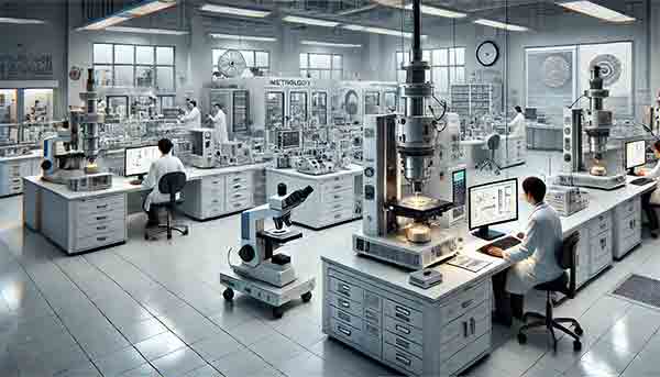
The metrology lab buzzed with a quiet intensity, the sound of low hums and occasional beeps from instruments punctuated by the muffled voices of research students. It was a sacred space for precise measurement and discovery—a place where technology and science converged to uncover truths invisible to the naked eye.
Sarah adjusted her lab coat and joined her team in front of the atomic force microscope (AFM). It was her turn to use the instrument, and she felt a mix of excitement and nervousness. Her research on nanoscale biosensors relied on accurate surface characterization, and today, the AFM would help her analyze the topography of her silicon-on-insulator (SOI) wafer.

"Make sure the tip is perfectly aligned," said Ravi, her mentor, leaning over her shoulder. He was a postdoc with a knack for troubleshooting even the most stubborn equipment.
Sarah carefully adjusted the cantilever under the microscope’s control screen. After a few tense moments, the image resolved on the monitor—a vivid three-dimensional map of the wafer’s surface. The nanoscale roughness was well within acceptable limits, confirming that her fabrication process had been successful.
Meanwhile, across the room, Alex was running an ellipsometer. His project focused on developing thin-film coatings for optical MEMS devices. He loaded a sapphire wafer into the stage, adjusting the instrument to measure the refractive index and thickness of the coating.
"How’s it looking?" asked Priya, his lab partner, who was analyzing data on a nearby computer.
"Good so far," Alex replied. "The coating’s thickness is around 290 nm, right in our target range. But the refractive index is a bit off—might need to adjust the deposition parameters."
Priya nodded, jotting notes in their shared lab journal. "Let’s compare these results to last week’s batch. If we see a trend, it might pinpoint the issue."
At another station, Miguel was calibrating the X-ray diffraction (XRD) machine to analyze the crystal structure of a fused quartz substrate. His research involved growing carbon nanotubes, and the XRD would confirm if the substrate’s crystal orientation matched his requirements for optimal growth.
"This substrate better be [1,0,0]," he muttered as the machine whirred to life. Moments later, peaks appeared on the graph displayed on the monitor. Miguel smiled; the distinct pattern confirmed the substrate orientation.
Over at the profilometer, Jasmine was measuring the step height of etched patterns on her silicon wafer. She was working on microelectrodes for a biosensor, and the uniformity of her etch depth was crucial for consistent electrical performance.
"Looks like a 10 nm variation across the wafer," she remarked, calling over Dr. Lee, the faculty advisor.
"Not bad," Dr. Lee said after examining the results. "But try tweaking the plasma etching recipe. A little more fine-tuning and you’ll be within spec."
In a corner of the lab, Liam was testing wafer flatness with the interferometer. He had been tasked with finding substrates for a new photonics project, and any deviation in flatness could distort optical alignment. As the interference fringes came into focus, he documented the subtle bowing in his sapphire wafer, pondering how helium backside cooling during processing might have contributed to the issue.
"Flatness is decent," Liam said to himself, "but I wonder if a different crystal plane orientation would hold up better under stress."
Nearby, a group of students gathered around the scanning electron microscope (SEM). Emily, a first-year PhD student, was using it to examine the cross-section of a deposited oxide layer. She carefully adjusted the magnification, marveling at the intricate details of the film.
"Whoa," said Ben, a senior researcher. "Look at those grain boundaries. You might have some uneven deposition in there."
"Really?" Emily frowned, taking notes. "Could that affect our device performance?"
"Possibly," Ben replied. "But let's measure the grain sizes and see how uniform they are before jumping to conclusions."
By lunchtime, the lab was filled with animated discussions. Students shared insights, debated anomalies, and brainstormed solutions over coffee and sandwiches. Each measurement revealed a piece of the puzzle, bringing their collective projects closer to fruition.
As the day wound down, Sarah returned to the AFM station to capture additional scans for her report. She felt a growing sense of pride and ownership over her work. The metrology lab wasn’t just about data; it was about understanding—translating numbers and graphs into meaningful conclusions that could advance science and technology.
When the lights dimmed and the instruments fell silent, the students left the lab with notebooks full of observations and heads brimming with ideas. The precision tools of the metrology lab had done their part, but it was the students’ creativity and curiosity that would transform raw data into innovation.
In the world of research, measurement wasn’t merely a task—it was the foundation of discovery. And in the metrology lab, the next breakthrough always felt within reach.